

All Products
-
Integrated Circuits (ICs)
- Integrated Circuits (ICs)
- AC to DC Converter ICs
- Active Filters
- ADC
- AFE
- Analog Multipliers & Dividers
- Analog Switches & Multiplexers ICs
- Application Specific Microcontrollers
- Application Specific Timer
- Audio Amplifiers
- Audio Special Purpose
- Battery Chargers ICs
- Battery Management ICs
- Buffers & Transceivers
- Capacitive Sensors
- Clock Buffers & Drivers
- Clock Generators
- CODECs Interface ICs
- Comparators
- Configuration Proms for FPGAs
- Controllers Interface ICs
- Converting Interface ICs
- Counters & Dividers
- CPLDs
- Current Regulator IC
- DAC
- DC DC Voltage Regulators
- DC to DC converter
- DDS
- Delay Lines Timing ICs
- Digital Potentiometers
- Display Drivers ICs
- Drivers Interface ICs
- DSP
- Embedded ICs Modules
- Energy Metering ICs
- FIFOs Memory
- Flip Flops
- FPGAs
- FPGAs with Microcontrollers
- Full & Half-Bridge Drivers ICs
- Gate Drivers ICs
- Gates & Inverters
- Hot Swap Controllers
- I/O Expanders
- IC Batteries
- Ideal Diode controller
- Instrumentational OP Amps
- Interface ICs Modules
- Laser Driver ICs
- Latches
- LED Driver ICs
- Lighting Controllers
- Linear Comparators
- Linear Regulator Controllers
- Linear Voltage Regulators
- Memory
- Memory Batteries
- Memory Controllers
- Microcontrollers
- Microprocessors
- Modems ICs & Modules
- Motor Drivers
- Multi-Functional Gates & Inverters
- Multivibrators
- Multivibrators
- PFC PMICs
- PLDs
- PoE Controllers
- Power Supply Control ICs
- Power Switches ICs
- Programmable Timers & Oscillators
- RMS to DC Converters
- RTCs
- Sensor & Detector Interface ICs
- Serializers & Deserializers
- Shift Registers
- Signal Buffers
- Signal Switches & Multiplexers
- Signal Terminators
- SoC
- Special Purpose ADCs/DACs
- Special Purpose Amplifiers
- Special Purpose Analog Switches
- Specialized ICs
- Specialized Interface ICs
- Specialized Power Management ICs
- Specialized Voltage Regulators
- Specialty Logic ICs
- Switching Voltage Regulators
- Telecom Interface ICs
- Thermal Management
- Touch Screen Controllers
- UARTs
- Universal Bus Functions
- V/F & F/V Converters
- Video Amps & Modules
- Video Processing Linear ICs
- Voice Record and Playback
- Voltage Reference
- Voltage Supervisors
- Voltage Translators & Level Shifters
-
Connectors
- Connectors
- ARINC Connectors
- Backplane Connector Contacts
- Backplane Connectors Accessories
- Backplane Connectors Housings
- Backshells and Cable Clamps
- Banana Tip Adapters
- Banana Tip Binding Posts
- Banana Tip Connectors Accessories
- Banana Tip Jacks
- Barrel Accessories
- Barrel Adapters
- Barrel Audio Connectors
- Barrel Connectors
- Barrel Power Connectors
- Barrier Terminal Blocks
- Between Series Adapters
- Blade Type Power Connectors
- Blade Type Power Connectors
- Blade Type Power Connectors Accessories
- Blade Type Power Connectors Housings
- Board In Connectors
- Board to Board Connectors
- Card Edge Adapters
- Card Edge Connectors Accessories
- Card Edge Connectors Housings
- Card Edge Contacts
- Centronics Connectors
- Circular Adapters
- Circular Connectors
- Circular Connectors Accessories
- Circular Connectors Housings
- Circular Contacts
- Coaxial Connectors
- Coaxial Connectors Accessories
- D-Sub Adapters
- D-Sub Connector Housings
- D-Sub Connector Terminators
- D-Sub Connectors
- D-Sub Connectors Accessories
- D-Sub Contacts
- D-Sub Hoods
- D-Sub Jackscrews
- DIN 41612 Connectors
- Din Rail Terminal Blocks
- Edgeboard Connectors
- Faceplates & Frames
- Fiber Optic Adapters
- Fiber Optic Connectors
- Fiber Optic Connectors Accessories
- Fiber Optic Connectors Housings
- Flat Flexible Connector Housings
- Flat Flexible Connectors
- Flat Flexible Connectors Accessories
- Flat Flexible Contacts
- Foil Connectors
- Hard Metric Connector
- Headers & Male Pins
- Heavy Duty Connectors Accessories
- Heavy Duty Connectors Assemblies
- Heavy Duty Connectors Frames
- Heavy Duty Connectors Housings
- Heavy Duty Connectors Modules
- Heavy Duty Contacts
- IC Adapters
- IC and Component Sockets
- IC Sockets Accessories
- Inline Memory Module Sockets
- Interface Modules Terminal Blocks
- Keystone Accessories
- Keystone Inserts
- Knife Connectors
- Leadframe Contacts
- LGH Connectors
- Magnetic Wire Terminals
- Magnetics Modular Jacks
- Memory Card Adapters
- Memory Card Sockets
- Memory Connectors Accessories
- Modular Adapters
- Modular Connectors Accessories
- Modular Jacks
- Modular Plug Housings
- Modular Plugs
- Multi Purpose Contacts
- Panel Mount Connectors
- Panel Mount Terminal Blocks
- PC Pin Terminals
- Photovoltaic Connectors
- Photovoltaic Connectors Accessories
- Photovoltaic Contacts
- Pluggable Connectors
- Pluggable Connectors Accessories
- Pluggable Terminal Blocks
- Power Distribution Terminal Blocks
- Power Entry Connectors Accessories
- Power Entry Connectors Modules
- Quick-Connect & Quick-Disconnect Connectors
- Rectangular Connectors
- Rectangular Connectors Accessories
- Rectangular Connectors Adapters
- Rectangular Connectors Arrays
- Rectangular Connectors Headers
- Rectangular Connectors Housings
- Rectangular Contact Inserts
- Rectangular Terminals
- RF Adapters
- RF Contacts
- RF Terminators
- Ring Terminals
- Screw Connectors
- Shunts & Jumpers
- Socket Terminals
- Solder Lug Connectors
- Spade Connectors
- Specialized Backplane Connectors
- Specialized Connectors
- Specialized Terminal Blocks
- Spring Loaded Contacts
- Spring Loaded Rectangular Connectors
- SSL Connectors
- SSL Connectors Accessories
- SSL Contacts
- Terminal Block Adapters
- Terminal Blocks - Contacts
- Terminal Blocks Accessories
- Terminal Jumpers
- Terminal Junction Systems
- Terminal Marker Strips
- Terminal Strips and Turret Boards
- Terminal Wire Ferrules
- Terminals Accessories
- Terminals Adapters
- Terminals Housings
- Transistor Sockets
- Turret Connectors
- Video Adapters
- Video Connector Accessories
- Video Connectors
- Wire Pin Connectors
- Wire Splice Connectors
- Wire-to-Board Connectors
- Wire-to-Board Terminal Blocks
- Wiring Blocks Accessories
- Wiring Modular Connectors
-
Discrete Semiconductors
- Discrete Semiconductors
- Arrays BJT Transistors
- BJT Transistors Arrays
- Bridge Rectifiers
- DIACs and SIDACs
- IGBTs Modules
- IGBTs Transistors Arrays
- JFETs Transistors
- MOSFETs Transistors Arrays
- Power Driver Modules
- Pre-Biased BJT Transistors
- Programmable Unijunction Transistors
- Rectifier Diode Array
- RF BJT Transistors
- RF Diodes
- RF MOSFETs Transistors
- SCRs Thyristors
- Single BJT Transistors
- Single IGBTs
- Single IGBTs
- Single MOSFETs Transistors
- Single-Phase Diode Rectifier
- Specialized Transistors
- Thyristors Modules
- TRIACs Thyristors
- Varactors
- Zener Diode Arrays
- Zener Single Diodes
-
Capacitors
- Capacitors
- Aluminum Electrolytic Capacitors
- Aluminum Polymer Capacitors
- Capacitor Accessories
- Capacitor Networks
- Ceramic Capacitors
- Ceramic Capacitors
- Film Capacitors
- Mica & PTFE Capacitors
- Niobium Oxide Capacitors
- Silicon Capacitors
- Supercapacitors & EDLC
- Tantalum Capacitors
- Tantalum Polymer Capacitors
- Thin Film Capacitors
- Trimmers Variable
-
Sensors
- Sensors
- CdS Cells
- Accelerometers
- Accessories
- Amplifiers
- Analog & Digital Sensor
- Analog & Digital Sensors
- Analog Optical Sensors
- Angle & Linear Position Measuring Sensors
- Camera Modules
- Color Sensors
- Current Sensors
- Distance Measuring Sensors
- Dust Sensors
- Encoders
- Float & Level Sensors
- Flow Sensors
- Force Sensors
- Gas Sensors
- Gyroscopes
- Humidity Sensors
- Image Sensors
- IMUs
- Inclinometers
- IrDA Transceiver Modules
- Junction Blocks
- Logic Optical Sensors
- Logic Photo Detectors
- Logic Photointerrupters
- LVDT Transducers
- Magnetic Compass Sensors Modules
- Magnetic Linear Sensors ICs
- Magnetic Position Sensors Modules
- Magnetic Switches
- Mechanical Temperature Sensors
- Multi Purpose Magnets
- Multifunction
- NTC Thermistors
- Occupancy Sensors
- Optical Motion Sensors
- Optical Sensors Remote Receiver
- Photodiodes
- Photoelectric Sensors
- Phototransistors
- Proximity Sensors
- PTC Thermistors
- RTD
- Sensor Cable Accessories
- Sensor Cable Assemblies
- Sensor Matched Magnets
- Shock Sensors
- Solar Cells
- Solid State Thermostats
- Specialized Sensors
- Strain Gauges
- Thermocouple Temperature Sensors
- Tilt Switch Sensors
- Touch Sensors
- Transducers
- Transistor Optical Sensors
- Ultrasonic Receivers
- UV Sensors
- Vibration Sensors
- Resistors
- Isolators
- Board Mount Poser Supplies
-
RF/IF & RFID
- RF/IF & RFID
- Attenuators
- Balun
- RF Accessories
- RF Amplifiers
- RF Antennas
- RF Boards
- RF Demodulators
- RF Detectors
- RF Directional Coupler
- RF Front End
- RF Misc ICs and Modules
- RF Mixers
- RF Modulators
- RF Multiplexers
- RF Power Controller ICs
- RF Power Dividers
- RF Receivers
- RF Shields
- RF Switches
- RF Transceiver ICs
- RF Transceiver Modules
- RF Transmitter
- RF Transmitters
- RFI & EMI Contacts
- RFI & EMI Materials
- RFID Accessories
- RFID Antennas
- RFID Boards
- RFID ICs
- RFID Reader Modules
- RFID Tags
- Circuit Protection
- Crystals
- Inductors
- Filters

LPC1766FBD100
You may place an order without registering to Utmel.
We strongly suggest you sign in before purchasing as you
can track your order in real time.
For your convenience, we accept multiple payment methods in USD, including PayPal, Credit Card, and wire transfer.
RFQ (Request for Quotations)It is recommended to request for quotations to get the latest
prices and inventories about the part.
Our sales will reply to
your request by email within 24 hours.
1. You'll receive an order information email in your inbox.
(Please remember to check the spam folder if you didn't hear from us).
2. Since inventories and prices may fluctuate to some
extent, the sales manager is going to reconfirm the order and let you know if there
are any updates.
Shipping starts at $40, but some countries will exceed $40. For
example (South Africa, Brazil, India, Pakistan, Israel, etc.)
The
basic freight (for package ≤0.5kg or corresponding volume) depends on the time zone and
country.
Currently, our products are shipped through DHL, FedEx, SF, and UPS.
Delivery TimeOnce the goods are shipped, estimated delivery time depends on the shipping methods you chose:
FedEx International, 5-7 business days.
The following are some common countries' logistic time.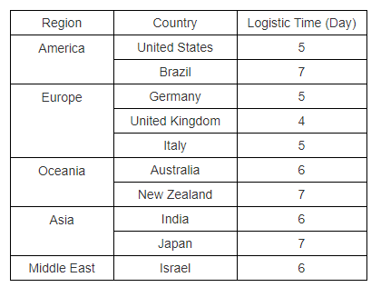
| Parameters | |
|---|---|
| Peripherals | DMA |
| Bit Size | 32 |
| Has ADC | YES |
| DMA Channels | YES |
| Number of Timers/Counters | 4 |
| Density | 2 Mb |
| CPU Family | ARM7 |
| Number of ADC Channels | 8 |
| ROM Programmability | FLASH |
| Number of PWM Channels | 6 |
| Number of GPIO | 70 |
| REACH SVHC | No SVHC |
| RoHS Status | RoHS Compliant |
| Package / Case | LQFP |
| Surface Mount | YES |
| Number of Pins | 100 |
| JESD-609 Code | e3 |
| Pbfree Code | yes |
| Moisture Sensitivity Level (MSL) | 3 |
| Number of Terminations | 100 |
| Termination | SMD/SMT |
| Terminal Finish | Tin (Sn) |
| Max Operating Temperature | 85°C |
| Min Operating Temperature | -40°C |
| Subcategory | Microcontrollers |
| Technology | CMOS |
| Terminal Position | QUAD |
| Terminal Form | GULL WING |
| Peak Reflow Temperature (Cel) | 260 |
| Supply Voltage | 3.3V |
| Terminal Pitch | 0.5mm |
| Frequency | 100MHz |
| Time@Peak Reflow Temperature-Max (s) | 30 |
| Pin Count | 100 |
| Qualification Status | Not Qualified |
| Power Supplies | 2.5/3.3V |
| Temperature Grade | INDUSTRIAL |
| Interface | CAN, I2C, SPI, SSP, UART |
| Max Supply Voltage | 3.6V |
| Min Supply Voltage | 2.4V |
| Memory Size | 256kB |
| Number of I/O | 70 |
| RAM Size | 64kB |
| uPs/uCs/Peripheral ICs Type | MICROCONTROLLER, RISC |
LPC1766FBD100 Decription
The LPC1766FBD100 is an embedded microcontroller for ARM Cortex-M3 applications that has a high level of integration and uses little power. A next-generation core, the ARM provides system improvements such improved debug tools and deeper support block integration. Up to 80 MHz of CPU frequency are supported by the LPC1766. The ARM Cortex-M3 CPU uses a Harvard architecture with a three-stage pipeline, independent local instruction and data buses, and a third bus for peripherals. Additionally, the inbuilt prefetch unit of the ARM Cortex-M3 CPU allows speculative branching. The LPC1766's peripheral complement consists of 4 UARTs, 2 CAN channels, 8-channel general-purpose DMA controller, Ethernet MAC, USB Device/Host/OTG interface, and kB of flash memory and kB of data memory. Two SSP controllers, three I2C interfaces, two inputs and two outputs on an I2S interface, an 8-channel 12-bit ADC, a 10-bit DAC, motor control PWM, a quadrature encoder interface, four general-purpose timers, six general-purpose outputs, an ultra-low power RTC with a separate battery supply, and up to 70 general-purpose I/O pins are all included. The ARM7-based LPC2366 microcontroller and the LPC1766 have pin compatibility.
There is a Memory Protection Unit (MPU) with support for eight regions. ARM Cortex-M3 built-in Nested Vectored Interrupt Controller (NVIC) (NVIC). 256 kB of on-chip flash memory for programming. A better flash memory accelerator enables 80 MHz operating at high speed with no wait states. Using the on-chip boot loader software, in-system programming (ISP) and in-application programming (IAP) are possible. SRAM on the CPU with a local code/data channel for high-performance CPU access is included in the 64 kB on-chip SRAM. Two 16 kB SRAM blocks with distinct access pathways for improved throughput. Along with serving as general-purpose CPU instruction and data storage, these SRAM blocks can also be used as Ethernet, USB, and DMA memory.
LPC1766FBD100 Features
Package: QFP100
RoHS: Lead free / RoHS Compliant
LPC1766FBD100 Applications
Industrial
Personal electronics
Communications equipment