

All Products
-
Integrated Circuits (ICs)
- Integrated Circuits (ICs)
- AC to DC Converter ICs
- Active Filters
- ADC
- AFE
- Analog Multipliers & Dividers
- Analog Switches & Multiplexers ICs
- Application Specific Microcontrollers
- Application Specific Timer
- Audio Amplifiers
- Audio Special Purpose
- Battery Chargers ICs
- Battery Management ICs
- Buffers & Transceivers
- Capacitive Sensors
- Clock Buffers & Drivers
- Clock Generators
- CODECs Interface ICs
- Comparators
- Configuration Proms for FPGAs
- Controllers Interface ICs
- Converting Interface ICs
- Counters & Dividers
- CPLDs
- Current Regulator IC
- DAC
- DC DC Voltage Regulators
- DC to DC converter
- DDS
- Delay Lines Timing ICs
- Digital Potentiometers
- Display Drivers ICs
- Drivers Interface ICs
- DSP
- Embedded ICs Modules
- Energy Metering ICs
- FIFOs Memory
- Flip Flops
- FPGAs
- FPGAs with Microcontrollers
- Full & Half-Bridge Drivers ICs
- Gate Drivers ICs
- Gates & Inverters
- Hot Swap Controllers
- I/O Expanders
- IC Batteries
- Ideal Diode controller
- Instrumentational OP Amps
- Interface ICs Modules
- Laser Driver ICs
- Latches
- LED Driver ICs
- Lighting Controllers
- Linear Comparators
- Linear Regulator Controllers
- Linear Voltage Regulators
- Memory
- Memory Batteries
- Memory Controllers
- Microcontrollers
- Microprocessors
- Modems ICs & Modules
- Motor Drivers
- Multi-Functional Gates & Inverters
- Multivibrators
- Multivibrators
- PFC PMICs
- PLDs
- PoE Controllers
- Power Supply Control ICs
- Power Switches ICs
- Programmable Timers & Oscillators
- RMS to DC Converters
- RTCs
- Sensor & Detector Interface ICs
- Serializers & Deserializers
- Shift Registers
- Signal Buffers
- Signal Switches & Multiplexers
- Signal Terminators
- SoC
- Special Purpose ADCs/DACs
- Special Purpose Amplifiers
- Special Purpose Analog Switches
- Specialized ICs
- Specialized Interface ICs
- Specialized Power Management ICs
- Specialized Voltage Regulators
- Specialty Logic ICs
- Switching Voltage Regulators
- Telecom Interface ICs
- Thermal Management
- Touch Screen Controllers
- UARTs
- Universal Bus Functions
- V/F & F/V Converters
- Video Amps & Modules
- Video Processing Linear ICs
- Voice Record and Playback
- Voltage Reference
- Voltage Supervisors
- Voltage Translators & Level Shifters
-
Connectors
- Connectors
- ARINC Connectors
- Backplane Connector Contacts
- Backplane Connectors Accessories
- Backplane Connectors Housings
- Backshells and Cable Clamps
- Banana Tip Adapters
- Banana Tip Binding Posts
- Banana Tip Connectors Accessories
- Banana Tip Jacks
- Barrel Accessories
- Barrel Adapters
- Barrel Audio Connectors
- Barrel Connectors
- Barrel Power Connectors
- Barrier Terminal Blocks
- Between Series Adapters
- Blade Type Power Connectors
- Blade Type Power Connectors
- Blade Type Power Connectors Accessories
- Blade Type Power Connectors Housings
- Board In Connectors
- Board to Board Connectors
- Card Edge Adapters
- Card Edge Connectors Accessories
- Card Edge Connectors Housings
- Card Edge Contacts
- Centronics Connectors
- Circular Adapters
- Circular Connectors
- Circular Connectors Accessories
- Circular Connectors Housings
- Circular Contacts
- Coaxial Connectors
- Coaxial Connectors Accessories
- D-Sub Adapters
- D-Sub Connector Housings
- D-Sub Connector Terminators
- D-Sub Connectors
- D-Sub Connectors Accessories
- D-Sub Contacts
- D-Sub Hoods
- D-Sub Jackscrews
- DIN 41612 Connectors
- Din Rail Terminal Blocks
- Edgeboard Connectors
- Faceplates & Frames
- Fiber Optic Adapters
- Fiber Optic Connectors
- Fiber Optic Connectors Accessories
- Fiber Optic Connectors Housings
- Flat Flexible Connector Housings
- Flat Flexible Connectors
- Flat Flexible Connectors Accessories
- Flat Flexible Contacts
- Foil Connectors
- Hard Metric Connector
- Headers & Male Pins
- Heavy Duty Connectors Accessories
- Heavy Duty Connectors Assemblies
- Heavy Duty Connectors Frames
- Heavy Duty Connectors Housings
- Heavy Duty Connectors Modules
- Heavy Duty Contacts
- IC Adapters
- IC and Component Sockets
- IC Sockets Accessories
- Inline Memory Module Sockets
- Interface Modules Terminal Blocks
- Keystone Accessories
- Keystone Inserts
- Knife Connectors
- Leadframe Contacts
- LGH Connectors
- Magnetic Wire Terminals
- Magnetics Modular Jacks
- Memory Card Adapters
- Memory Card Sockets
- Memory Connectors Accessories
- Modular Adapters
- Modular Connectors Accessories
- Modular Jacks
- Modular Plug Housings
- Modular Plugs
- Multi Purpose Contacts
- Panel Mount Connectors
- Panel Mount Terminal Blocks
- PC Pin Terminals
- Photovoltaic Connectors
- Photovoltaic Connectors Accessories
- Photovoltaic Contacts
- Pluggable Connectors
- Pluggable Connectors Accessories
- Pluggable Terminal Blocks
- Power Distribution Terminal Blocks
- Power Entry Connectors Accessories
- Power Entry Connectors Modules
- Quick-Connect & Quick-Disconnect Connectors
- Rectangular Connectors
- Rectangular Connectors Accessories
- Rectangular Connectors Adapters
- Rectangular Connectors Arrays
- Rectangular Connectors Headers
- Rectangular Connectors Housings
- Rectangular Contact Inserts
- Rectangular Terminals
- RF Adapters
- RF Contacts
- RF Terminators
- Ring Terminals
- Screw Connectors
- Shunts & Jumpers
- Socket Terminals
- Solder Lug Connectors
- Spade Connectors
- Specialized Backplane Connectors
- Specialized Connectors
- Specialized Terminal Blocks
- Spring Loaded Contacts
- Spring Loaded Rectangular Connectors
- SSL Connectors
- SSL Connectors Accessories
- SSL Contacts
- Terminal Block Adapters
- Terminal Blocks - Contacts
- Terminal Blocks Accessories
- Terminal Jumpers
- Terminal Junction Systems
- Terminal Marker Strips
- Terminal Strips and Turret Boards
- Terminal Wire Ferrules
- Terminals Accessories
- Terminals Adapters
- Terminals Housings
- Transistor Sockets
- Turret Connectors
- Video Adapters
- Video Connector Accessories
- Video Connectors
- Wire Pin Connectors
- Wire Splice Connectors
- Wire-to-Board Connectors
- Wire-to-Board Terminal Blocks
- Wiring Blocks Accessories
- Wiring Modular Connectors
-
Discrete Semiconductors
- Discrete Semiconductors
- Arrays BJT Transistors
- BJT Transistors Arrays
- Bridge Rectifiers
- DIACs and SIDACs
- IGBTs Modules
- IGBTs Transistors Arrays
- JFETs Transistors
- MOSFETs Transistors Arrays
- Power Driver Modules
- Pre-Biased BJT Transistors
- Programmable Unijunction Transistors
- Rectifier Diode Array
- RF BJT Transistors
- RF Diodes
- RF MOSFETs Transistors
- SCRs Thyristors
- Single BJT Transistors
- Single IGBTs
- Single IGBTs
- Single MOSFETs Transistors
- Single-Phase Diode Rectifier
- Specialized Transistors
- Thyristors Modules
- TRIACs Thyristors
- Varactors
- Zener Diode Arrays
- Zener Single Diodes
-
Capacitors
- Capacitors
- Aluminum Electrolytic Capacitors
- Aluminum Polymer Capacitors
- Capacitor Accessories
- Capacitor Networks
- Ceramic Capacitors
- Ceramic Capacitors
- Film Capacitors
- Mica & PTFE Capacitors
- Niobium Oxide Capacitors
- Silicon Capacitors
- Supercapacitors & EDLC
- Tantalum Capacitors
- Tantalum Polymer Capacitors
- Thin Film Capacitors
- Trimmers Variable
-
Sensors
- Sensors
- CdS Cells
- Accelerometers
- Accessories
- Amplifiers
- Analog & Digital Sensor
- Analog & Digital Sensors
- Analog Optical Sensors
- Angle & Linear Position Measuring Sensors
- Camera Modules
- Color Sensors
- Current Sensors
- Distance Measuring Sensors
- Dust Sensors
- Encoders
- Float & Level Sensors
- Flow Sensors
- Force Sensors
- Gas Sensors
- Gyroscopes
- Humidity Sensors
- Image Sensors
- IMUs
- Inclinometers
- IrDA Transceiver Modules
- Junction Blocks
- Logic Optical Sensors
- Logic Photo Detectors
- Logic Photointerrupters
- LVDT Transducers
- Magnetic Compass Sensors Modules
- Magnetic Linear Sensors ICs
- Magnetic Position Sensors Modules
- Magnetic Switches
- Mechanical Temperature Sensors
- Multi Purpose Magnets
- Multifunction
- NTC Thermistors
- Occupancy Sensors
- Optical Motion Sensors
- Optical Sensors Remote Receiver
- Photodiodes
- Photoelectric Sensors
- Phototransistors
- Proximity Sensors
- PTC Thermistors
- RTD
- Sensor Cable Accessories
- Sensor Cable Assemblies
- Sensor Matched Magnets
- Shock Sensors
- Solar Cells
- Solid State Thermostats
- Specialized Sensors
- Strain Gauges
- Thermocouple Temperature Sensors
- Tilt Switch Sensors
- Touch Sensors
- Transducers
- Transistor Optical Sensors
- Ultrasonic Receivers
- UV Sensors
- Vibration Sensors
- Resistors
- Isolators
- Board Mount Poser Supplies
-
RF/IF & RFID
- RF/IF & RFID
- Attenuators
- Balun
- RF Accessories
- RF Amplifiers
- RF Antennas
- RF Boards
- RF Demodulators
- RF Detectors
- RF Directional Coupler
- RF Front End
- RF Misc ICs and Modules
- RF Mixers
- RF Modulators
- RF Multiplexers
- RF Power Controller ICs
- RF Power Dividers
- RF Receivers
- RF Shields
- RF Switches
- RF Transceiver ICs
- RF Transceiver Modules
- RF Transmitter
- RF Transmitters
- RFI & EMI Contacts
- RFI & EMI Materials
- RFID Accessories
- RFID Antennas
- RFID Boards
- RFID ICs
- RFID Reader Modules
- RFID Tags
- Circuit Protection
- Crystals
- Inductors
- Filters

UCC21530QDWKRQ1
You may place an order without registering to Utmel.
We strongly suggest you sign in before purchasing as you
can track your order in real time.
For your convenience, we accept multiple payment methods in USD, including PayPal, Credit Card, and wire transfer.
RFQ (Request for Quotations)It is recommended to request for quotations to get the latest
prices and inventories about the part.
Our sales will reply to
your request by email within 24 hours.
1. You'll receive an order information email in your inbox.
(Please remember to check the spam folder if you didn't hear from us).
2. Since inventories and prices may fluctuate to some
extent, the sales manager is going to reconfirm the order and let you know if there
are any updates.
Shipping starts at $40, but some countries will exceed $40. For
example (South Africa, Brazil, India, Pakistan, Israel, etc.)
The
basic freight (for package ≤0.5kg or corresponding volume) depends on the time zone and
country.
Currently, our products are shipped through DHL, FedEx, SF, and UPS.
Delivery TimeOnce the goods are shipped, estimated delivery time depends on the shipping methods you chose:
FedEx International, 5-7 business days.
The following are some common countries' logistic time.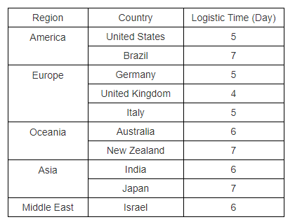
| Parameters | |
|---|---|
| Logic Voltage - VIL, VIH | 1.2V 1.6V |
| Built-in Protections | TRANSIENT; UNDER VOLTAGE |
| Output Current Flow Direction | SOURCE SINK |
| Length | 10.3mm |
| Width | 7.5mm |
| RoHS Status | ROHS3 Compliant |
| Mounting Type | Surface Mount |
| Package / Case | 14-SOIC (0.295, 7.50mm Width) |
| Surface Mount | YES |
| Operating Temperature | -40°C~130°C TJ |
| Packaging | Tape & Reel (TR) |
| Series | Automotive, AEC-Q100 |
| JESD-609 Code | e4 |
| Pbfree Code | yes |
| Part Status | Obsolete |
| Moisture Sensitivity Level (MSL) | 3 (168 Hours) |
| Number of Terminations | 14 |
| Terminal Finish | Nickel/Palladium/Gold (Ni/Pd/Au) |
| Voltage - Supply | 3V~18V |
| Terminal Position | DUAL |
| Terminal Form | NO LEAD |
| Number of Functions | 1 |
| Supply Voltage | 3.3V |
| Base Part Number | UCC21530 |
| JESD-30 Code | S-PDSO-N14 |
| Input Type | CMOS/TTL |
| Output Current-Max | 6A |
| Rise / Fall Time (Typ) | 6ns 7ns |
| Interface IC Type | BUFFER OR INVERTER BASED PERIPHERAL DRIVER |
| Channel Type | Independent |
| Number of Drivers | 2 |
| Supply Voltage1-Nom | 15V |
| Driven Configuration | Half-Bridge |
| Gate Type | IGBT, N-Channel, P-Channel MOSFET |
| Current - Peak Output (Source, Sink) | 4A 6A |
Description
The UCC21530QDWKRQ1 is a 4-A source and 6-A sink peak current isolated dual-channel gate driver. It's made to drive IGBTs, Si MOSFETs, and SiC MOSFETs at up to 5-MHz with the best propagation delay and pulse-width distortion in the industry.
A 5.7-kVRMS reinforced isolation barrier isolates the input side from the two output drivers, providing common-mode transient immunity of at least 100 V/ns (CMTI). A working voltage of up to 1850 V can be achieved thanks to internal functional isolation between the two secondary-side drivers.
This driver can be set up as two low-side drivers, two high-side drivers, or a half-bridge driver with adjustable dead time (DT). When the EN pin is pulled low, it shuts down both outputs at the same time, however when it is left open or pulled high, it allows normal functioning. Primary-side logic faults require both outputs to be low as a fail-safe strategy.
VDD supply voltages of up to 25 V are accepted by the device. The driver is suited for interfacing with both analog and digital controllers due to its wide input VCCI range of 3 V to 18 V. Under-voltage lock-out (UVLO) protection is present on all supply voltage pins.
Features
? Programmable overlap and dead time
? Rejects input pulses and noise transients shorter than 5 ns
? Operating temperature range –40 to +125°C
? Safety-related certifications:
– 8000-VPK isolation per DIN V VDE V 0884-11 :2017-01
– 5.7-kVRMS isolation for 1 minute per UL 1577
– CSA certification per IEC 60950-1, IEC 62368-1, IEC 61010-1 and IEC 60601-1 end equipment standards
– CQC certification per GB4943.1-2011
? Common-mode transient immunity (CMTI) greater than 100-V/ns
? Isolation barrier life >40 years
? 4-A peak source, 6-A peak sink output
? TTL and CMOS compatible inputs
? 3-V to 18-V input VCCI range
? Up to 25-V VDD output drive supply
– 8-V and 12-V VDD UVLO options
? AEC-Q100 qualified with:
– Device temperature grade 1
– Device HBM ESD classification level H2
– Device CDM ESD classification level C6
? Functional Safety Quality-Managed
– Documentation available to aid functional safety system design
? Universal: dual low-side, dual high-side or half-bridge driver
? Wide body SOIC-14 (DWK) package
? 3.3-mm spacing between driver channels
? Switching parameters:
– 19-ns typical propagation delay
– 10-ns minimum pulse width
– 5-ns maximum delay matching
– 6-ns maximum pulse-width distortion
Applications
? AC inverter and servo drive
? AC-to-DC and DC-to-DC power delivery
? Energy storage systems
? HEV and BEV battery chargers
? Solar string and central inverters
? AC-to-DC and DC-to-DC charging piles